Laser cutting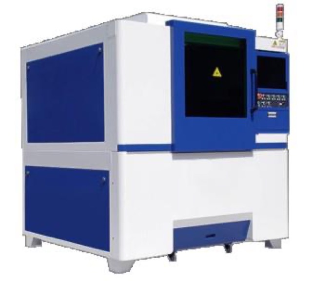
Board Cutting Machine
- TypeFiber laser
- Kerf0.05–0.15 mm
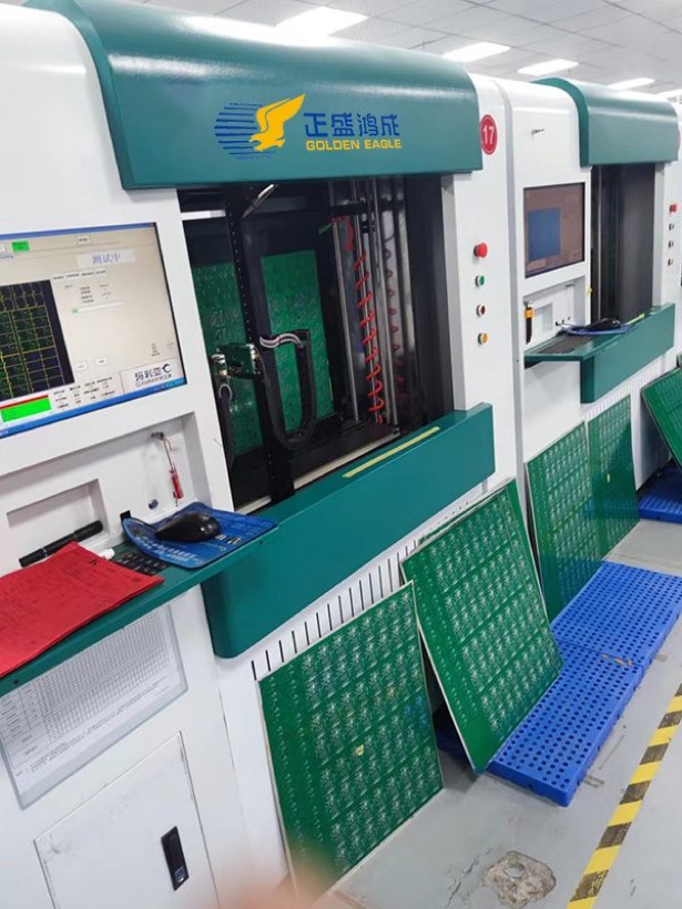
GE-LCB6080 — cuts copper / aluminum PCB with no mechanical stress or burr. View specs →
The complete chain of PCB machines, grouped in the order a board moves through the shop — cutting and drilling, plating, image transfer, etching, solder mask, surface finish and final test — for single, double-sided and multilayer boards and FPC.
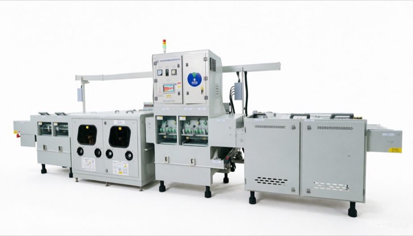
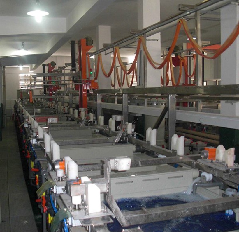
GE builds equipment for every stage of PCB fabrication. Below, the machines are organised by process flow — the real sequence of a production line — so you can see which unit does each job and configure a turnkey line end to end. Our horizontal spray PCB etching machines run both ferric chloride (FeCl₃) and regenerable cupric chloride (CuCl₂) chemistries, with conveyor speed and spray pressure tuned for even, repeatable copper etching across the whole panel.
From laminate to tested board — tap a step to jump to the machines used in that stage.
Cut the copper-clad laminate to size and make every hole — laser cutting leaves no stress or burr, CNC routers drill and profile, and the target driller sets multilayer registration.
GE-LCB6080 — cuts copper / aluminum PCB with no mechanical stress or burr. View specs →
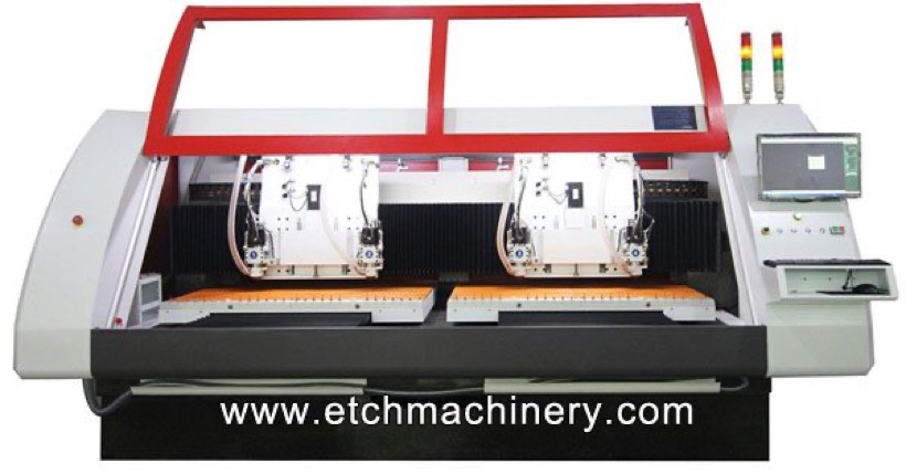
Multi-spindle CNC for through-holes and board-outline profiling.
Drills tooling / target holes for accurate multilayer layer-to-layer alignment.
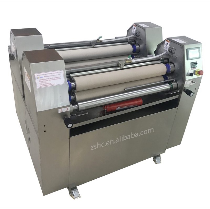
After drilling, the panel is deburred, brushed and washed so the copper is clean and slightly roughened — the condition dry film and plating need to adhere.
Removes drill burrs and conditions the copper surface for resist and plating adhesion.
Drilled holes are chemically metallized, then copper is electroplated onto the holes and tracks so double-sided and multilayer boards conduct through the board.
Electroless copper through-hole metallization plus copper electroplating on holes and pattern.
Transfer the circuit (and later the solder-mask) pattern: apply resist, expose the artwork, and develop to reveal the copper that will be etched. See the full exposure machine range.
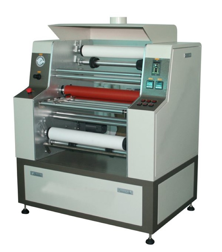
Laminates dry film or coats liquid photoresist evenly before exposure.
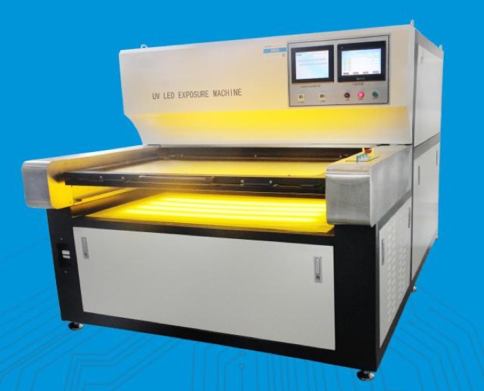
Single / double-side, 4-CCD / 8-CCD and LDI — open the full exposure range. View specs →

Develops the exposed resist to reveal the copper pattern ahead of etching.
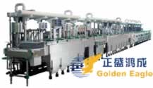
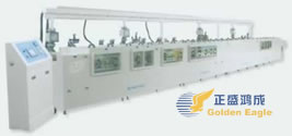
The core step — the etching machine dissolves the bare copper to leave the circuit, the regeneration system keeps the etchant at constant strength, and the stripper removes the resist.

Dissolves bare copper to leave the circuit, with even etch across the whole panel.
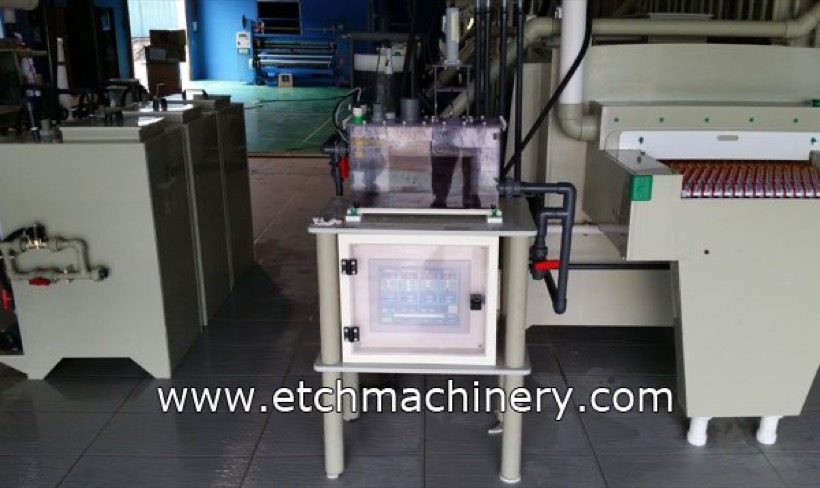
Holds the etchant at constant concentration, steadying etch rate and cutting chemical cost.

Removes the dry-film resist or solder mask cleanly after etching.
Coat the board with solder-mask ink, expose and develop it (reusing the exposure / developing line), print the legend marking, and bake to cure between wet steps.
Applies solder-mask ink evenly across one or both sides of the board.
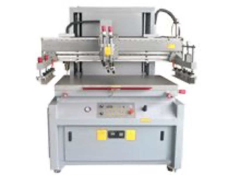
Prints legend (silkscreen) marking and screen inks onto the panel.
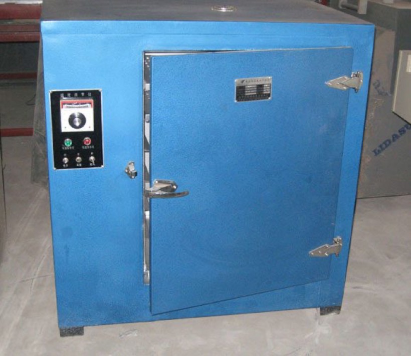
Bakes and cures ink and dries panels between the wet process steps.
Finish the exposed copper pads so they stay solderable — choose hot-air solder leveling, organic OSP, or electroless nickel / immersion gold for fine-pitch and BGA.
Coats the pads with solder and levels them flat with hot air knives.
Organic solderability preservative that keeps copper pads solderable and flat.
Electroless nickel + immersion gold for a flat, durable, wire-bondable finish.
Bring the board to final form — V-groove scoring for depaneling, a final clean, electrical test, and automatic loading / unloading to link the line.
Cuts V-grooves so panels snap apart cleanly at depaneling.
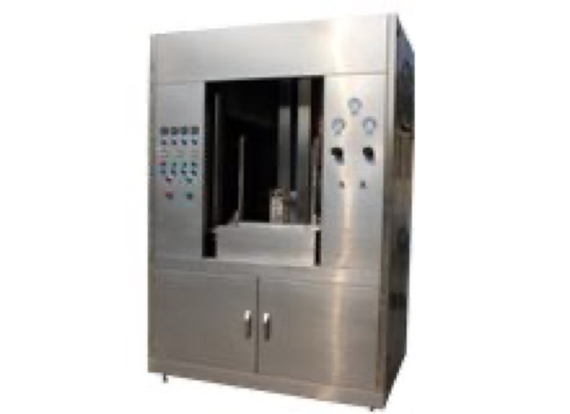
Final wash and dry of the finished board before inspection and packing.
Fixtureless electrical test of opens and shorts — ideal for prototype and small batch.
Automatic board loading and unloading to connect line stages and cut handling.
Tell us your board size, layer count, copper weight and monthly volume — we'll configure the right PCB machines stage by stage, from cutting to final test.