LDI Laser Direct Imaging Exposure Machine
A laser direct imaging (LDI) exposure machine that writes circuit and solder-mask patterns directly from data with no phototool — for fine-line, HDI and quick-turn PCB.
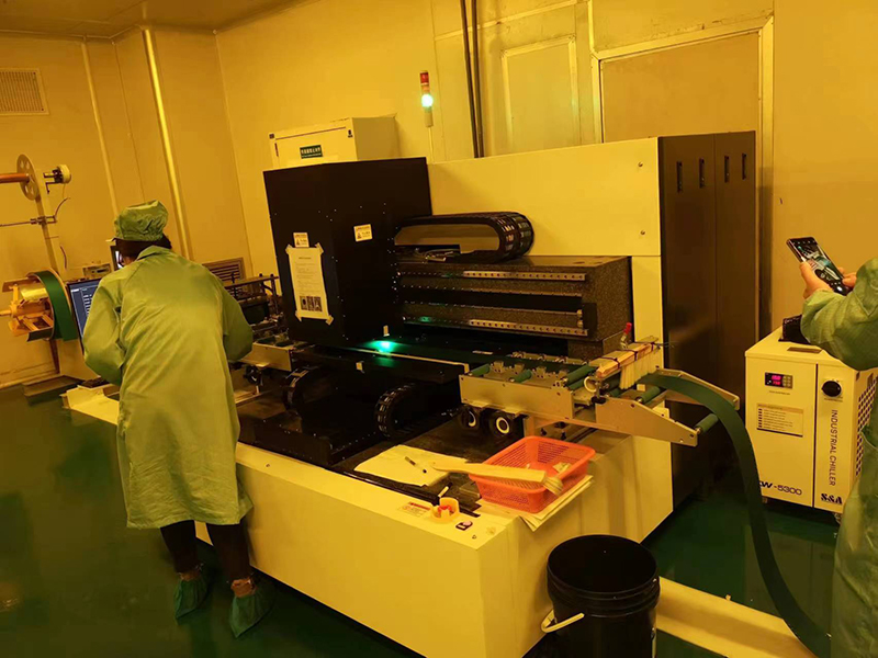
No film — image straight from your data
LDI throws out the film. Instead of printing a phototool and contact-exposing it, the GE-LDI500 scans a 405nm laser / DMD image straight onto the dry film or solder-mask ink from your Gerber data. Because there is no film, there is no film cost, no registration loss from film stretch, and design changes go live immediately — ideal for quick-turn and prototype runs. Cameras read the panel fiducials and the image is warped to match each board, so registration holds to a few microns even on slightly distorted panels. Line resolution reaches the 25µm class, which is why LDI has become the standard for fine-line and HDI work.
- ModelGE-LDI500
- MethodLaser direct imaging, filmless
- Light source405nm laser / DMD digital head
- Resolution≤ 25 µm line/space class
- AlignmentDynamic fiducial, auto image warp
- Registration± 5 µm class
- MaterialDry film & solder-mask ink
- Best forFine-line, HDI, quick-turn PCB
- Data inGerber / direct from CAM
Why go filmless
No phototool
No film cost, no film storage.
Instant design change
Edit data, expose — no re-film.
Dynamic alignment
Image warps to each panel.
≤25µm lines
Fine-line and HDI capable.
No film-stretch error
Registration not lost to film.
Quick-turn ready
Prototype and short runs fast.
LDI Laser Direct Imaging Exposure Machine — common questions
Laser Direct Imaging — a laser/DMD writes the circuit or solder-mask pattern directly onto the resist from your CAM data, with no photographic film or contact frame.
No film cost or storage, instant design changes, and no registration error from film stretch or contact — plus finer lines (25µm class) for HDI. It pays off most on fine-line and quick-turn work.
Cameras read each panel's fiducials and the system warps the projected image to match the real board, so registration holds to a few microns even on slightly distorted or scaled panels.
Inner/outer-layer circuit dry film and solder-mask ink, straight from Gerber/CAM — the same steps the contact and CCD machines do, but without a phototool.